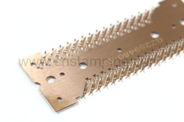
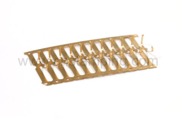
Chip Packaging and Testing Clips in Semiconductor Industry
Definition of Chip Packaging and Testing Clips
Chip packaging and testing clips are that after the chip is completely sealed, the seal manufacturer will test the quality and reliability of the chip product to see if it meets the customer’s standards. Quality inspection mainly detects the availability of the chip after packaging, as well as the quality and performance of the package. The reliability is the test of the reliability-related parameters of the package. At this time, the packaging and testing clips will be used.
Since the clips needs frequent work in chip sealing testing, all packaging and testing factories have certain requirements for the production of clips for chip packaging and testing.
The metal clips from our factory has below advantages:
Long lifetime: up to 200,000 times;
Resistance of Insertion & extration: more than 10,000 times;
Positivity: 0.05mmmax;
Verticality: 0.05mmmax;
Straightness: 10mm;
Standard: 0.05mmmax.
The clips for chip packaging and testing requires long lifetimes. We can choose suitable materials from raw materials, or use surface treatment to increase the life of the workpiece.

Packaging Methods of Chip Packaging and Testing Clips
Chip packaging and testing clip is the contact medium for chip testing, which is an important part of electronic materials and a carrier of electrical components. Its function is through the clips conductive transmission function body data to judge whether the product is normal contact and normal operation data, as a kind of data transmission and conductive contact.
It is suitable for testing the adhesion of gold and aluminum wires in various seal forms of semiconductors. And for COB sealing, optoelectronics, led, SMT Assembly, and adhesion testing of originals and substrates.
The packaging methods has three ways, such as package in PET bags, in a tube and in a reel bag. It can be made into rolls. People also call this kind of packaging as carrier tape packaging or disk packaging. It is mostly used in automated production, which can save a lot of time, but the price is much higher.
The above is the commonly packaging method for chip test clips. Also, we can package it according to customer requirements.

Heat Treatment
People mainly use Chip packaging and testing clips in various optical communication and consumer electronics chip aging tests and packaging test fixtures. It is also needs to be heat-treated after production. As it can improve the hardness, wear resistance and contact fatigue strength of the surface of the testing clips, and improve the strength and toughness of the core.
However, the chip packaging and testing clips will encounter the workpiece is turn black and discolored in the process of vacuum heat treatment. So, How to prevent and deal with this situation?
It is very simple. That is to increase the process of cleaning and degreasing before heat treatment, so as to avoid blackening and discoloration as much as possible.
![]()
After years of research in the field of precision stamping processing, Dongguan Heju Precision Electronic Technology Co., Ltd. has reached long-term cooperation with many Fortune 500 companies. It has brand imported punching press equipment, and the accuracy of metal contacts and terminals is high (the punching accuracy can up to +/- 0.01 mm), and the max punching speed can reach 1500SPM. Please feel free to contact us to learn more informations.
