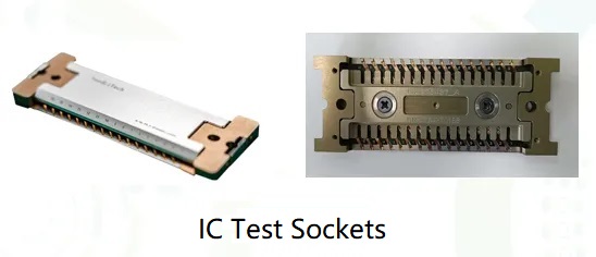
Semiconductor Test Socket Pins Manufacturer
A test socket is a crucial element in Semiconductor product development and testing. Different types of test sockets are needed for different testing processes with specialized electrical and mechanical parameters. For a high performance test socket, the contactors, the pins in the socket, play a very important role in transferring the signal between the device under test (DUT) and the system with the least amount of signal attenuation or degradation.

IC Packaging&Testing Socket Pins/Contact Terminals
Heju Stamping has 30yrs stamping experience in the design and manufacturing of semiconductor precision stamping parts. Such as semiconductor test socket pins, Burn-in&Test socket contact terminals, chip package metal contacts, etc.
To meet different demands for testing, Hejustamping provides the industry with wide variety of semiconductor test socket pins solutions with great design flexibility.
Performance Index of Test Socket Pins
100 Million Times
Lifetime of Socket Pins
1 Million Times
Insert and Extract Times
Accuracy ±0.005mm
Accuracy of Socket Pins
±0.05
Verticality Tolerence (mm)
±0.05
Straightness
(based on 10mm)
How We do
1) To ensure the parts the same as drawing and meet the function of elastic, Heju using a dozen of operations to forming step by step, and doing some special treatment for bending mold part.
2) Using axiliary bridge structure layout design to ensure the parts’ dimension stable.

Our Critical Controling Points
-
Spring Contacts
commission test -
Raw Material
hardness test, elongation test, tensile strength test, yield strength test -
After Plating
salt spray test, coating thickness test, high temperature aging test
Frequently Asked Questions
How to ensure the life time of spring contacts?
The life time of micro spring contacts can reach 10-100 thousand times. To ensure the life time, Heju stamping will make material or contacts heat treat.In that way, hardness can keep in 36-52 HRC.
How to solve the problem of large size and small size?
The abrasion of punching cutter,material deformation can lead to the punching hole to large or too small.In practice, Heju stamping will find a solution to the problem according to the specific circumstances.such as: Material testing,regular maintenance of mold parts etc.
How to choose the material to ensure the performance of contact springs?
To ensure the performance,we usually choose the ECuSn-C with high hardness, toughness and good corrosion resistance. The ECuSn-C contact can ensure 500,000 times life at least.Except the material, the thickness, technology process and others can influence the performance and life time.
How to avoid the elastic part of the spring to produce greater stress (rebound)?
While forming,most of contacts need bending process.If curvature radius is too small, the bending parts will produce large rebound.So the curvature radius must be 5 times larger than the thickness of the material at least.
© Copyright 2012 - 2023 CNstamping All rights reserved.
